
Table of Contents >> Show >> Hide
- Capacitive Touch in Plain English
- Before You Open Eagle: Three Decisions That Save Hours
- Layout Rules That Matter More Than Your Font Choice
- Eagle Workflow: Turning “Touch Pad” Into Copper That Behaves
- Example 1: A Dead-Simple Touch Button (Self-Cap)
- Example 2: A Slider or Wheel (Mutual Cap) Without the Pain
- Debugging: When Your Touch UI Thinks It’s a Paranormal Investigator
- Eagle Gotchas That Specifically Bite Capacitive Sensors
- Production Notes: Make It Robust, Not Just “Working”
- Conclusion
- Real-World Shop Notes: of “I Wish Someone Told Me”
Capacitive touch feels like magic until you remember it’s basically your finger acting like a tiny, noisy,
water-filled antenna. The “magic” part is making that antenna behave on a PCB that’s also packed with clocks,
switching regulators, LEDs, and the occasional gremlin (also known as EMI).
This guide shows how to design easy capacitive touch sensors in Eagle (Autodesk EAGLE / Fusion
Electronics) without turning your board into a haunted piano. You’ll learn the electrode shapes that tend to work,
how to use polygons and keepouts the right way, and which layout details actually move the needleespecially for
buttons, sliders, and wheels.
Capacitive Touch in Plain English
Capacitive touch sensing measures small changes in capacitance caused by a finger approaching or touching an
electrode. The electric field “fringes” out from the copper into the air and through your overlay (plastic, glass,
acrylic). When a finger gets close, the field lines shift and the measured capacitance changes. Your controller
(MCU, dedicated touch IC, or sensor front-end) turns that tiny change into a reliable “touch” event by sampling,
filtering, and applying thresholds.
Self-capacitance vs. mutual-capacitance
You’ll run into two main architectures:
-
Self-capacitance (single electrode): each button is one pad. It’s simpler and great for single
keys and basic UIs. It can be more sensitive to environmental changes and large nearby objects. -
Mutual-capacitance (X/Y electrodes): touch is detected by how a finger changes coupling between
interleaved or crossing electrodes. This is common for sliders, wheels, and touchpads because it can provide
better position resolution and noise performance in many designs.
In Eagle terms: self-cap touch is “draw a pad and route a trace.” Mutual-cap is “draw a tiny comb made of copper,
then draw another comb, and do it consistently 12 times without crying.” We’ll make it doable.
Before You Open Eagle: Three Decisions That Save Hours
1) Know your overlay and stack-up
The cover material (acrylic, glass, ABS), its thickness, and whether there’s an air gap matter as much as pad size.
A button that works perfectly under 1 mm plastic can feel dead under 4 mm. If you’re prototyping, pick an overlay
early and keep it consistent across revisions so you’re not “tuning” a moving target.
2) Pick your sensing silicon (and be honest about your schedule)
If you want the quickest path, use a dedicated controller like the MPR121 or a simple one-channel part like an
AT42QT101x-style device, or choose an MCU with a mature touch library. If your project needs sliders/wheels or
liquid tolerance, consider a platform with strong reference designs and tooling.
3) Define “works” in real life
Touch in a quiet lab is easy. Touch near a motor, charger, LED drivers, or a long cable is where layout matters.
Decide now: Will it be used with wet hands? Gloves? In a kitchen? Near strong EMI? That determines whether you can
keep the PCB simple or you need shielding, better grounding strategy, and more robust filtering.
Layout Rules That Matter More Than Your Font Choice
Electrode size and shape: start practical
For basic buttons, simple shapes (circle, rounded rectangle) are forgiving. A common starting point is a button
around the size of a fingertip (think roughly 10–15 mm across), then adjust based on overlay thickness and your
controller’s sensitivity settings.
For mutual-cap keys, interleaved “fingers” increase coupling area while keeping geometry compact. The trick is
consistency: equal finger widths, equal spacing, and repeatable patterns across all channels so your firmware
tuning doesn’t become a one-off science fair project.
Keep noisy copper away from the sensor (yes, even ground sometimes)
Ground is a friend… until it’s too close. A big solid ground plane directly under a self-cap pad can increase
parasitic capacitance and reduce sensitivity. Many proven designs use a hatched ground or a
carefully controlled shield strategy around/behind sensors. Your goal is controlled return paths and controlled
parasiticsnot “pour ground everywhere and hope.”
Route sense traces like they’re allergic to switching edges
- Keep the sense trace short and direct.
- Keep it away from high dV/dt nets: clocks, USB, SMPS nodes, LED PWM, motor lines.
- Avoid running parallel to noisy traces for long distances.
- Try to keep similar channels similar in length and routing style when practical.
Use simple protection and stable components
Touch channels can be ESD magnets because they’re literally designed to be near humans. Many reference designs
recommend sensible ESD protection approaches and emphasize stable capacitors and clean power for repeatable
measurements.
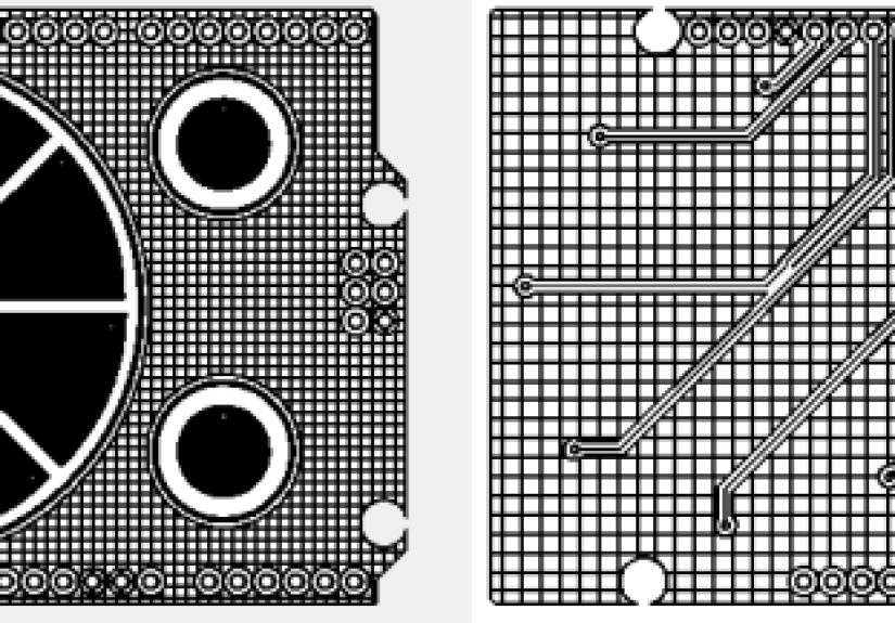
Eagle Workflow: Turning “Touch Pad” Into Copper That Behaves
Eagle is excellent at drawing exactly what you ask foreven when what you ask for accidentally creates tiny gaps,
odd polygon ranks, and a copper pour that silently ruins sensitivity. Here’s a workflow that stays sane.
Step 1: Draw the electrode on the correct copper layer
For a simple self-cap button, you can use a POLYGON on Top (or Bottom) and name
it like a net (e.g., TOUCH1). A polygon makes it easy to create rounded shapes and consistent clearances.
- Use a comfortable grid (e.g., 0.5 mm) so your shapes are clean.
- Prefer rounded corners; sharp corners can concentrate fields and invite EMI/ESD trouble.
- Once drawn, use NAME to assign it to the touch net.
- Run RATSNEST to pour polygons and confirm you got the intended geometry.
Step 2: Create a keepout so “helpful” copper doesn’t sneak under your pad
If you don’t want copper under a sensor on a layer, create an area on the appropriate restrict/keepout layer.
In Eagle, that often means using tRestrict / bRestrict (and sometimes
tKeepout / bKeepout, depending on your flow) to prevent pours or routing from
entering an area. A classic method is to draw a polygon on the restrict layer covering the “no copper” zone.
Practical tip: make the keepout slightly larger than the pad so you don’t end up with a thin ground “halo” hiding
under your overlay and stealing sensitivity.
Step 3: Add a controlled ground strategy (hatched pour or guard geometry)
Many touch references recommend a ground strategy that balances shielding and sensitivity. In Eagle, you can make a
ground polygon and set it to HATCH pour style with an isolation gap that keeps it from crowding
the electrode. You can also form a perimeter “guard” concept using ground copper around the sensor region,
especially when you care about ESD behavior.
Eagle knobs that matter here:
- ISOLATE: clearance between polygon and other copper.
- RANK: which polygon wins when pours overlap.
- THERMALS: often disabled for sensor electrodes so the shape is solid and predictable.
- POUR: solid vs hatch, depending on your design goal.
Step 4: Route the sense trace and place the “boring” parts close
If your design uses a series resistor, place it close to the sensing pin. If your controller uses a sampling
capacitor or recommends particular dielectric stability, follow that guidance and keep the capacitor placement
tight. In practice, touch circuits behave better when the analog-ish parts are close and the routing is calm.
Example 1: A Dead-Simple Touch Button (Self-Cap)
Let’s design a single button that works through a plastic overlay:
- Electrode: draw a 12 mm diameter circular polygon on Top, name it
TOUCH1. - Keepout: draw a slightly larger circle on
tRestrictto block ground pours under it. - Sense trace: route from the pad to your IC/MCU pin, avoiding noisy nets.
- Ground strategy: pour a hatched ground around (not under) the electrode to help with ESD and noise control.
- Overlay test: tape your intended overlay material on top and test sensitivity before you commit.
If you’re using a breakout-style controller, many guides show you can attach an external electrode with a wire or
copper tape and still detect touch through common plastics. That’s a great way to prototype electrode size before
you lock your PCB layout.
Example 2: A Slider or Wheel (Mutual Cap) Without the Pain
For a slider, you typically interleave X and Y electrodes. A straightforward pattern is:
- X electrodes: repeating “fingers” connected together into one net.
- Y electrodes: alternating “fingers” connected into another net.
- Spacing and width: keep them consistent and manufacturable.
Eagle approach:
-
Draw one “cell” of interleaved fingers using polygons or wires on the Top copper layer.
Duplicate it across the slider length with consistent spacing. - Name all X shapes to
X0and all Y shapes toY0(or however your controller maps channels). -
If your design guide suggests splitting X and Y across layers to adjust coupling/parasitics, you can put X on Top
and Y on an inner layer or Bottomthen use keepouts and careful stack-up to keep the coupling consistent. -
Pour ground thoughtfully around the slider region. Avoid accidental copper under the active coupling zone unless
your reference design explicitly calls for a shield plane or driven shield strategy.
Wheels are basically sliders that took a yoga class and learned how to bend. The same rules applyrepeatable
geometry, consistent spacing, and clean routing.
Debugging: When Your Touch UI Thinks It’s a Paranormal Investigator
Symptom: Random touches when the charger is plugged in
This usually points to noise coupling into the sense trace or ground reference shifting. Solutions often include:
better separation from switching nodes, improved power decoupling, changing ground strategy near sensors, or using
firmware filtering and re-tuning thresholds for the actual operating condition (charging).
Symptom: Works on the bench, fails in the enclosure
Metal brackets, batteries, displays, and even a nearby ground plane inside the product can change parasitics.
If the enclosure adds a big conductive surface near the electrode, your baseline capacitance can jump and your
delta shrinks. Fixes may include resizing the electrode, adjusting keepouts, rethinking shield/ground placement,
or using driven shield techniques when supported.
Symptom: One button is “weak” compared to the others
Often it’s trace length, routing proximity to noisy nets, or an inconsistent ground pour nearby. The fastest fix:
make that channel’s layout look like the good channels. Firmware can compensate to a point, but consistent hardware
is the gift that keeps on giving.
Eagle Gotchas That Specifically Bite Capacitive Sensors
-
Open contours: if your polygon boundary isn’t truly closed, Eagle may not pour it the way you
expect. Zoom in and check for tiny gaps at corners. -
Polygon rank surprises: overlapping polygons can lead to a ground pour creeping into a region you
thought was protected. Set ranks intentionally, then verify with RATSNEST. -
Thermals on electrodes: a sensor pad that accidentally gets thermal spokes can behave differently
(and look sloppy). Consider disabling thermals for the electrode polygon. -
Inconsistent keepouts across layers: you might block copper on Top but forget Bottom or an inner
layer. If you’re using 4 layers, check all relevant copper layers for accidental parasitics.
Production Notes: Make It Robust, Not Just “Working”
A touch UI that ships needs to survive ESD events, humidity shifts, and manufacturing variation. Good practices:
- ESD strategy: plan the discharge path and keep sensitive nodes protected.
- Stable materials: keep overlay thickness and adhesive consistent in production.
- Test points: include a way to measure or log touch baselines during validation.
- Firmware tuning hooks: even great hardware benefits from tuning in the final enclosure.
Conclusion
“Easy capacitive touch sensors in Eagle” isn’t about a single magic shapeit’s about controlling the stuff you can
control: electrode geometry, parasitic capacitance, routing, and ground strategy. Eagle gives you the tools:
polygons, keepouts, ranks, and pours. Pair those with proven touch-layout habits and you’ll spend more time
enjoying your UI and less time arguing with a button that only works when the moon is in retrograde.
Real-World Shop Notes: of “I Wish Someone Told Me”
The first time I drew a capacitive button in Eagle, I did what any confident human would do: I made a gorgeous
copper circle, poured a heroic ground plane everywhere, routed the sense trace right past a PWM LED line, and then
acted shocked when the “button” triggered every time the LEDs dimmed. My takeaway: touch sensing is basically
analog design wearing a digital costume.
The second surprise was how often the problem wasn’t the padit was the stuff near the pad. In one build,
two buttons behaved perfectly and one was mushy. Same size, same code, same controller. The “bad” button happened
to have a longer sense trace that ran parallel to a clock line for about 30 mm. In Eagle, the route looked clean.
On the scope (and in the touch logs), it looked like my button was listening to a techno station.
Shortening that trace and giving it distance fixed it more than any firmware tweak.
Another lesson: keepouts are not optional decoration. I once assumed, “It’s fine if ground is under the pad; more
ground is more better.” Then the overlay thickness changed late in the game (prototype acrylic was thinner than
the production panel). Suddenly the button needed more sensitivityexcept the big plane underneath had already
inflated parasitic capacitance so much that there wasn’t much sensitivity left to buy. Creating a real keepout
zone under the electrode (and verifying every layer) gave me back headroom.
The most “Eagle-specific” pain point was polygon behavior. A sensor electrode that looked like a closed shape at
normal zoom wasn’t closed at allone tiny corner didn’t meet. Eagle poured something, but not what I thought.
The board “kinda worked,” which is the most dangerous kind of working because you’ll waste days tuning software to
compensate for a geometry bug. Now I do a ritual: zoom in, confirm boundaries, run RATSNEST, and visually inspect
the copper as if I’m looking for Waldo.
I also learned to prototype electrodes fast. Before locking the PCB, I’ll often try two or three pad sizes on the
same board (even if the UI only needs one). It feels like overkill until you realize it’s cheaper than respinning
a board because your “perfect” 9 mm button is allergic to winter humidity. Prototyping variations turns touch from
“mystery” into “engineering.”
Finally, don’t underestimate the enclosure. A metal standoff, a battery can, or even a conductive label behind the
panel can shift your baselines. I’ve had a design pass every bench test and then fail when mounted because the
internal metal bracket sat just close enough to the sensor region to change the field. Now, I test early in the
real mechanical stack-upeven if it means a scrappy 3D-printed jigbecause “works on the bench” is not a shipping
requirement.
If all of this sounds dramatic, good: it means you’ll respect touch sensing just enough to keep it simple.
Draw clean electrodes, control the copper around them, route like you’re avoiding trouble (because you are),
and verify pours and keepouts like your future self is paying you a consult fee.