
Table of Contents >> Show >> Hide
- Quick Diagnosis: Is It Really a Broken Trace?
- Prep Work: The 10 Minutes That Save the Board
- Method 1: The Solder Bridge (A Tiny Puddle with a Big Warning Label)
- Method 2: The Wire Jumper (The “Most Reliable” Fix for Most Repairs)
- Method 3: Copper Foil Patch (When You Need a “Flat Trace,” Not a “Flying Wire”)
- Method 4: Conductive Ink or Silver Pen (For Delicate or Low-Heat Repairs)
- Method 5: Reroute to the Next Via (Plus Lifted Pad Survival Tactics)
- How to Choose the Right Repair Method
- Inspection and Bring-Up: Don’t Skip the Boring Part
- Common Mistakes That Make Repairs Fail
- How to Avoid Breaking Traces in the First Place
- Final Thoughts
- Experience Notes: What Typically Happens on the Bench (And What People Learn)
A broken PCB trace is the electronics equivalent of a broken shoelace: the rest of the outfit might be perfect,
but you’re not going anywhere until that one tiny line is back doing its job. The good news? You usually don’t
need a new board, a new gadget, or a new personality. You need a plan, a steady hand, and just enough patience
to not “fix” the problem into a second, more expensive problem.
Hackaday famously showcased several practical ways to repair broken PCB tracesfrom quick solder bridges to
neatly formed jumper wires and protective overcoats. Let’s take that spirit and turn it into a clear, in-depth,
real-world guide you can use at your bench (or kitchen table… no judgment, but maybe wipe the crumbs away).
Quick Diagnosis: Is It Really a Broken Trace?
Before you start scraping solder mask like you’re trying to uncover ancient treasure, confirm you actually have
a trace problem. “Dead board” symptoms can come from a blown fuse, failed component, cracked solder joint, or
corrosion. A broken trace is just one suspect in a crowded lineup.
Signs you may have a broken trace
- Visible crack, burn mark, or lifted copper along a trace or pad.
- Device works only when flexed, pressed, or held “just right” (a classic intermittent connection).
- A fuse keeps blowingor someone replaced the fuse with “whatever fit,” and now the trace is the fuse.
- Continuity test fails between two points that should be connected.
Two-minute confirmation with a multimeter
- Unplug power and discharge any large capacitors (especially in power supplies).
- Set your meter to continuity mode (or low-ohms).
- Probe the two ends of the suspected net (pad-to-pad, via-to-via, or component leg-to-leg).
- No beep (or “OL”)? You’ve likely found the break.
Prep Work: The 10 Minutes That Save the Board
PCB trace repair is 30% “making a new conductor” and 70% “making sure it actually sticks, solders, and survives.”
Most failures come from skipping prep: dirty copper, not enough exposed trace, weak mechanical support, or
forgetting to protect the repair afterward.
Tools that make life easier
- Magnification (a cheap loupe is better than squinting yourself into a headache).
- Sharp hobby knife or fiberglass pen for scraping solder mask.
- Flux (yes, even if you “hate sticky things”cleaning comes later).
- Fine soldering tip, temperature-controlled iron, solder wick, and isopropyl alcohol.
- Kapton tape and a small amount of epoxy or UV-curable solder mask/overcoat.
Step 1: Expose the copper
Most modern PCBs have solder mask covering traces. You’ll need clean copper to attach anything.
Carefully scrape away mask on both sides of the break. Aim for a few millimeters of exposed copper on each end,
not a microscopic pinprick that refuses to wet with solder.
Step 2: Clean and tin
Clean the exposed copper with isopropyl alcohol. Apply flux and tin the exposed ends with a thin layer of solder.
Tinning turns “fussy bare copper” into “friendly solderable landing pads.” If you end up with a big blob, wick
it backflat and tidy is the goal.
Method 1: The Solder Bridge (A Tiny Puddle with a Big Warning Label)
The fastest repair is to bridge a very small gap with solder. It’s tempting because it feels like you’re done in
five seconds. It can workespecially on low-current, low-stress repairsbut solder alone is not the most reliable
long-term conductor for a gap that might flex or heat-cycle.
When it makes sense
- The gap is extremely short (think hairline crack or tiny nick).
- The trace is relatively wide and not carrying heavy current.
- The board won’t be flexed or vibrated in normal use.
How to do it without regretting it
- Expose and tin both sides of the gap.
- Flood the gap with flux.
- Use a small amount of solder to connect the two tinned ends.
- Inspect under magnification for cold joints or accidental bridges to nearby traces.
- Protect it (UV solder mask, epoxy overcoat, or a proper conformal coating).
Pro tip: If you can, reinforce the solder bridge with a tiny strand of wire laid across the break before soldering.
That way, if the solder cracks later, the wire can still maintain continuity.
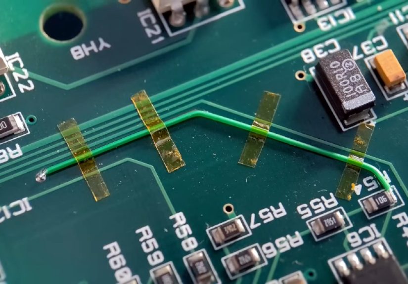
Method 2: The Wire Jumper (The “Most Reliable” Fix for Most Repairs)
If PCB trace repair had a “default setting,” it would be a wire jumper. It’s robust, electrically solid, and works
for short or long gaps. This is the approach many rework guides favor: replace the missing conductor with a known
conductor (wire), and secure it so it can’t rip off later.
Best wire choices
- 30 AWG Kynar wire-wrap wire: great for small signals and tight spaces.
- Enamel-coated magnet wire: excellent for fine work; the insulation can be removed by scraping or heat/flux.
- Solid core copper: good for short, sturdy jumpers; less forgiving if the board flexes.
- Heavier gauge: for power traces, choose wire that matches the original trace’s current needs.
Step-by-step jumper repair
- Expose and tin a few millimeters of copper on both ends of the break.
- Measure the route. For longer repairs, mimic the trace path to avoid creating accidental antennas or snag points.
- Cut and pre-tin the wire ends. If it’s insulated, strip a small section on each end.
- Solder one end to the first tinned pad/trace area.
- Form the wire to the board so it lies flat and follows a sensible path.
- Secure the wire with Kapton tape temporarily, then epoxy/overcoat for strain relief.
- Solder the other end and inspect carefully.
- Clean flux residue and test continuity.
Want a neat-looking repair? A fun trick highlighted in the Hackaday write-up is to “prototype the shape” with solder:
place small solder blobs to mark bends/turns, then use that as a guide to bend a clean jumper that hugs the original
route. Is it electrically necessary? No. Is it satisfying? Extremely.
Strain relief is not optional
A jumper wire floating in the air is an invitation for vibration to do what vibration does best: ruin your day.
Tack it down with a dot of epoxy or a protective overcoat. Your future self will thank you.
Method 3: Copper Foil Patch (When You Need a “Flat Trace,” Not a “Flying Wire”)
Copper foil (or copper tape) is ideal when the original conductor was wide, when you’re repairing a pad area,
or when you want the repair to stay low-profile. Done well, it can look surprisingly close to the original board layout.
Where copper foil shines
- Repairing wider traces (power rails, ground runs).
- Replacing a missing section of copper that peeled up with the solder mask.
- Rebuilding a damaged pad “landing area” (sometimes in combination with epoxy).
How to do a copper foil repair
- Scrape mask and clean the area thoroughly.
- Cut a foil strip matching the trace width (slightly longer than the damaged area).
- Lay the foil in place and tack it so it won’t slide.
- Solder the foil ends to the tinned copper on each side of the break.
- Check continuity and ensure the foil doesn’t short adjacent traces.
- Seal with overcoat/solder mask to protect against peeling and corrosion.
If your copper tape has conductive adhesive, treat it as “helpful positioning glue,” not your primary electrical
connection. The reliable connection should be the soldered joint at the ends (and any designed overlap).
Method 4: Conductive Ink or Silver Pen (For Delicate or Low-Heat Repairs)
Conductive ink feels like cheatingin a good way. You literally redraw the missing connection. For tiny gaps,
fragile boards, or places where you really don’t want to apply much heat, a conductive pen can be a practical solution.
Best use cases
- Very small breaks on fine traces where soldering would be risky.
- Quick restoration of continuity on low-current signal lines.
- Repairing traces on surfaces where a jumper wire would be awkward.
How to apply conductive ink correctly
- Expose copper on both ends of the break and clean thoroughly.
- Shake/prime the pen so the conductive material is well mixed.
- Draw the trace across the gap with a steady hand (thin and controlled beats thick and messy).
- Let it cure fully (often at least an hour, sometimes longer depending on product).
- Test continuity and resistance (not just “beep”some repairs can be resistive).
- Protect it with an overcoat or solder mask substitute to prevent wear and oxidation.
Limitations to respect
Conductive ink repairs can be more fragile than copper-and-solder repairs, and the resistance may be higher than a
real copper trace. Avoid using ink for high-current paths, flexing areas, or anything that gets hot. Think “signal fix,”
not “power highway.”
Method 5: Reroute to the Next Via (Plus Lifted Pad Survival Tactics)
Sometimes the trace is gone, the pad is lifted, or the copper is so damaged that attaching to it feels like trying to
build a bridge on Jell-O. In those cases, stop chasing the missing copper and reroute the connection to a solid point:
the next via, the next pad on the same net, or even the component leg that the trace ultimately connects to.
The “follow the net” approach
- Identify the net’s next reliable anchor point (via, test pad, connector pin, or component leg).
- Verify with continuity testing that the anchor point is indeed connected to where you need to go.
- Run a jumper wire from the original location (or component lead) to the anchor point.
- Secure the jumper with epoxy/overcoat to prevent fatigue.
Repairing a lifted pad (functional, not fancy)
Lifted pads often happen during desoldering: the copper pad detaches from the board substrate. If the pad is gone,
you usually can’t “glue it back into being a pad” and expect reliability. Instead:
- Scrape solder mask off the attached trace and solder the component lead directly to that exposed trace.
- If that’s not possible, follow the trace to the next via and jumper to there.
- In worst cases, jumper directly to the nearest component leg on the same net.
This method is less about making the board look new and more about making the circuit electrically correct again.
If you want pretty, you can always tidy it later with proper overcoat and careful routing.
How to Choose the Right Repair Method
The “best” trace repair depends on how much copper is missing, how much current flows, and how much abuse the board
will see after you put it back together.
| Situation | Best Starting Choice | Why |
|---|---|---|
| Tiny nick / hairline break | Solder bridge (or wire-reinforced solder) | Fast and effective if the gap is minimal. |
| Moderate break / missing segment | Wire jumper | Strong, reliable, and easy to inspect/test. |
| Wide power trace damaged | Copper foil patch (or heavier jumper) | Better cross-section for current, low profile. |
| Delicate board / low-heat needed | Conductive ink + overcoat | Minimal thermal stress, quick continuity restore. |
| Pad lifted / copper gone | Reroute to via or component leg | Anchors to solid points when the original pad can’t be trusted. |
Inspection and Bring-Up: Don’t Skip the Boring Part
The repair isn’t finished when it “looks connected.” It’s finished when it tests correctly, won’t short later, and can
survive normal use.
Checklist before power
- Continuity test across the repaired net.
- Short test to nearby traces/pads (especially if you scraped mask in a crowded area).
- Mechanical check: tug gently with tweezersnothing should lift.
- Clean flux residue (helps prevent corrosion and weird leakage paths).
- Overcoat or mask the repair to prevent oxidation and accidental shorts.
Power-up safely
If you can, use a current-limited bench supply. Start at the correct voltage with a conservative current limit.
Watch for sudden current spikes, heat, or smoke (the three classic signs of “oops”). After a minute or two,
gently touch near the repair area (or use a thermal camera if you’re fancy) to confirm it isn’t heating abnormally.
Common Mistakes That Make Repairs Fail
- Not enough exposed copper: solder sticks to solder, not to solder mask.
- No strain relief: the wire becomes a spring, then a crack, then a mystery intermittent.
- Overheating: lifted pads often start as “I just needed two more seconds.”
- Using conductive ink for power paths: it may work… until it doesn’t.
- Skipping cleaning: flux residue can trap grime, attract moisture, and cause leakage.
How to Avoid Breaking Traces in the First Place
Prevention is cheaper than repair (and also less dramatic).
- Use proper desoldering tools (wick, solder sucker, hot air) instead of brute force.
- Add fresh solder/flux before removing old soldercounterintuitive, but it improves flow.
- Let joints cool between attempts; repeated heat cycles weaken the copper-to-substrate bond.
- Support wires and connectors mechanically so they don’t yank on pads.
- Don’t “upgrade” fuses with higher ratings unless you like turning traces into fuses.
Final Thoughts
Broken PCB traces look intimidating because the damage is small and the stakes feel high. But most trace repairs boil
down to a simple idea: restore electrical continuity with a reliable conductor, then protect it mechanically and
environmentally. Whether you choose a solder bridge, a jumper wire, copper foil, conductive ink, or a reroute to the next
via, the winning move is always the same: careful prep, clean execution, and thorough testing.
Experience Notes: What Typically Happens on the Bench (And What People Learn)
Since electronics repair is a contact sport between humans and tiny copper lines, certain “bench experiences” show up
again and againespecially for hobbyists and first-time reworkers. Consider this section a field guide to the most common
moments that cause people to either level up… or sigh loudly and order a replacement board.
First: the “invisible break under the solder mask.” The board looks fine, the trace looks unburned, and the only clue is
that the device works when you flex it. Many repairers learn (the hard way) that solder mask can hide hairline cracks.
A continuity test across multiple points along the traceprobing from pad to via to component legoften reveals the exact
spot where continuity disappears. The lesson: don’t trust your eyes alone; the multimeter is the adult in the room.
Second: the “lifted pad domino effect.” People try to remove a stubborn through-hole component by heating one leg for too
long, then wiggling the part. The pad lifts. Then the next pad lifts. Then the part finally comes out, and the board now
looks like a tiny copper tornado went through it. Many techs eventually adopt a calmer workflow: add flux, add fresh solder,
desolder properly, and let the board cool between attempts. If a pad does lift, the most reliable fix is usually not
“gluing it back,” but instead following the trace to the next via and running a jumper to a solid anchor point.
Third: “conductive ink confidence… followed by conductive ink humility.” A silver pen repair can be wonderfully fast, and
on a low-current signal line it may last a long time. But people often discover that the ink line can scratch, crack, or
develop higher resistance if it isn’t protected. The common upgrade path is simple: once it tests good, cover it with an
overcoat or solder mask substitute so it can’t be rubbed off by a stray screwdriver, a cable, or the universe’s
inexplicable desire to cause shorts.
Fourth: “the jumper that became an antenna.” A long, looping jumper wire can pick up noise, couple into nearby signals,
or just physically interfere with reassembly. This tends to show up when someone repairs a trace on a high-impedance or
sensitive line and routes the jumper like a decorative ribbon. The experienced habit is to keep jumpers short, flat, and
sensiblefollowing the original trace route when practical, and securing the wire so it can’t move. Neatness isn’t just
aesthetics; it’s often reliability.
Fifth: “the repair that worked… until the case was screwed back on.” This is the classic moment where everything tests
fine on the bench, but reassembly presses the jumper against a shield can, another pad, or the metal case. The fix is not
magicjust insulation and planning. A small dab of epoxy for strain relief, a protective overcoat, or even carefully placed
Kapton tape can prevent the ‘reassembly short’ that turns victory into a mystery.
The big takeaway from real-world trace repair experiences is that the electrical connection is only half the job. The other
half is mechanical and environmental: will this survive vibration, handling, heat, and the next person opening the device?
When you treat a trace repair like a tiny piece of wiring harness worksecure it, protect it, test ityou get results that
last far longer than a “quick blob and pray” approach.