Table of Contents >> Show >> Hide
- What Is Electrical Discharge Machining, Really?
- Why EDM Sounds Brilliant for PCB Prototyping
- How It Compares With Traditional PCB Prototyping Methods
- The Famous EDM-PCB Experiment That Got People Talking
- Where EDM Has Real Advantages for Prototype Boards
- Why EDM Is Still a Tough Sell for Serious PCB Work
- Best Use Cases for Prototyping PCBs With EDM
- Design Advice if You Are Exploring the Concept
- The Big Verdict: Clever, Useful, but Not a Board-House Assassin
- Experience Notes: What Working Around This Idea Usually Teaches You
- Conclusion
Printed circuit board prototyping has always attracted a certain kind of person: the kind who sees a clean copper-clad panel and immediately thinks, “Yes, but what if I attacked this with science?” For decades, the usual choices have been chemical etching, CNC milling, perfboard improvisation, or sending Gerbers to a board house and refreshing the tracking page like it is a sports score. Then along comes a wonderfully weird idea: what if you could prototype PCBs with electrical discharge machining, or EDM?
It sounds a little outrageous because, frankly, it is. EDM is usually associated with precision metalworking, mold making, hardened tool steel, and industrial machines that look like they cost more than your car, your desk, and your coffee habit combined. PCB prototyping, on the other hand, usually lives in the world of copper-clad laminate, tiny traces, solder mask envy, and mild frustration. Put those two worlds together, and you get one of the most interesting “this might be genius or madness” fabrication ideas in recent memory.
This article takes a deep look at prototyping PCBs with electrical discharge machining: how the idea works, why makers and engineers find it appealing, where it can outperform traditional approaches, and where it still runs into the stubborn laws of materials, manufacturing, and basic reality. Because as cool as sparks are, they do not automatically grant production-ready boards.
What Is Electrical Discharge Machining, Really?
Electrical discharge machining is a manufacturing process that removes material using controlled electrical sparks rather than a spinning cutter or drill. In traditional EDM, an electrode and a conductive workpiece are separated by a tiny gap, usually inside a dielectric fluid. When the voltage conditions are right, a spark jumps the gap, eroding a microscopic amount of material. Repeat that thousands of times, and you can shape metal with impressive precision.
In normal industry use, EDM is prized for machining hard, conductive materials, cutting intricate shapes, producing tight tolerances, and avoiding the cutting forces that come with conventional machining. That last part matters. No cutting forces means no tiny end mill screaming for mercy, no dramatic tool deflection, and less mechanical stress on delicate features. In manufacturing terms, EDM is the calm chaos option.
There are several major EDM families. Wire EDM uses a continuously fed wire electrode to cut through conductive stock. Sinker EDM uses a shaped electrode to burn a cavity into a part. Hole-drilling EDM makes very small or deep holes. All of them rely on one uncompromising rule: the workpiece must be conductive. That rule is the first plot twist in the PCB story.
Why EDM Sounds Brilliant for PCB Prototyping
A standard PCB starts with an insulating base material, often FR-4, covered in thin copper. The copper is conductive. The substrate underneath is not. That means EDM cannot treat the whole board like a chunk of steel, but it can interact with the copper layer on the surface.
That insight is what makes the concept so compelling. Instead of chemically dissolving unwanted copper or mechanically milling isolation paths, an EDM-style approach can theoretically burn away narrow gaps in the copper itself. In other words, you are not carving the board in the traditional sense. You are using sparks to break electrical continuity where you do not want copper to remain.
For prototype builders, the appeal is obvious:
- No wet etching chemistry setup.
- No fragile micro end mills to snap in dramatic fashion.
- Potentially less fiberglass dust than aggressive milling.
- A lightweight toolhead, because the electrode does not need to push like a cutter.
- A fascinating route for fast isolation cuts on one-off boards.
That is the elevator pitch, anyway. And it is a very good elevator pitch. The problem is that elevators, unlike fabrication experiments, do not usually throw sparks.
How It Compares With Traditional PCB Prototyping Methods
Chemical Etching
Chemical etching remains a classic PCB fabrication method because it can produce detailed circuit patterns with strong repeatability. A resist protects the copper you want to keep, and the etchant removes what is exposed. It is precise and proven, but it also involves chemicals, disposal concerns, cleanup, and more process handling than many hobbyists want on a kitchen table that still hopes to host dinner later.
CNC PCB Milling
PCB milling physically removes copper to isolate traces. It is popular for rapid prototyping because it skips chemical waste and can be great for quick iterations. But the technique comes with real tradeoffs: tool wear, burrs, limits on multilayer work, and the constant need for precision in height control. Those tiny milling bits are not exactly known for emotional resilience.
Professional Board House Fabrication
For tiny components, repeatable quality, plated through-holes, solder mask, silkscreen, and multilayer work, a real PCB fabricator is still the gold standard. Commercial boards are manufactured through a specialized process that integrates imaging, etching, drilling, masking, plating, and finishing in ways a home setup simply does not match. Fast-turn PCB services have become so accessible that many engineers now reserve DIY methods for immediate experiments, not final validation boards.
That leaves EDM in an unusual niche: not replacing professional fabrication, but potentially offering an alternative to rough one-off prototyping when speed, curiosity, and unconventional tooling matter.
The Famous EDM-PCB Experiment That Got People Talking
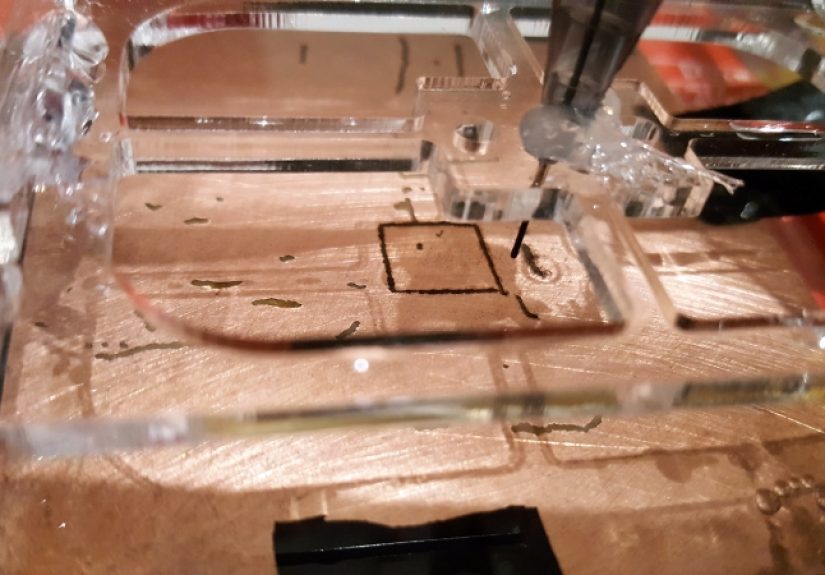
The idea gained attention through a well-known maker experiment that explored using a graphite electrode, including pencil lead, to cut isolation paths into copper-clad PCB stock. The concept was deliciously simple: bring a conductive electrode into light contact with the copper under the right electrical conditions, create controlled arcing, and let the discharge remove copper where needed.
What made the project especially interesting was not just that it worked at all, but that it revealed a set of highly practical observations. Graphite performed better than metal electrodes, which had a tendency to weld to the copper. Light contact mattered; too much force caused shorting instead of effective cutting. Cutting in water improved the quality of the cut, reinforcing what industrial EDM already knows: dielectric conditions and debris removal are a huge part of process stability.
In other words, the experiment did not merely shout “Look, sparks!” It showed that EDM-style PCB prototyping could produce real isolation cuts while also exposing the very process-control issues that would make automation difficult.
Where EDM Has Real Advantages for Prototype Boards
The strongest case for EDM-based PCB prototyping is not that it beats every other method. It is that it solves a very particular pain point: making quick, early-stage conductive patterns without heavy cutting forces or chemical baths.
That can be useful in several situations.
1. Low-Force Fabrication
Traditional milling pushes on the board. EDM does not. That means the machine can be lighter, the tool can be thinner, and workholding can be simpler. For experimental desktop systems, that is a major advantage.
2. Cheap Electrode Material
Graphite electrodes are inexpensive compared with specialized micro-milling tooling. When the consumable is basically glorified pencil lead, the tool budget becomes a lot less terrifying.
3. Fast Concept Iteration
For coarse-pitch, single-sided ideas where you want to test routing logic or simple electrical behavior, EDM-style isolation may be “good enough” much faster than a full fab cycle. Not pretty enough for a product launch, but plenty useful for answering, “Does this actually work?”
4. Reduced Dependence on Wet Chemistry
One reason people continue exploring alternative PCB prototyping methods is to avoid chemical handling. EDM offers a path that leans more on electrical control than chemical processing, which is attractive from both convenience and mess-avoidance standpoints.
Why EDM Is Still a Tough Sell for Serious PCB Work
Now for the less romantic part. EDM only works on conductive material, and a PCB is not a nice, thick, uniformly conductive block. It is a very thin copper layer bonded to an insulating substrate. That makes process control much trickier than it is in conventional metal EDM applications.
The Copper Is Thin
PCB copper is measured in ounces and mils, and it is often quite thin. That is great for circuit design, but not ideal when you are trying to control spark erosion with consistency. A process that is too aggressive can overcut, roughen edges, or damage what you meant to keep.
Electrode Wear Is Real
EDM electrodes wear during machining. In industrial systems, that is a managed variable. In a DIY PCB setup, it becomes part of the accuracy problem. If the electrode changes shape as it works, your cut width and trace isolation can drift.
The Substrate Changes the Game
FR-4 is an excellent insulator and the most common PCB substrate, which is part of why it is so widely used. But because the base material is non-conductive, you are not machining a stable conductive volume. You are interacting with a thin surface conductor over an insulator. That makes spark behavior less forgiving than it would be in a solid metal workpiece.
You Still Do Not Get the “Real PCB” Extras
Even if the copper pattern comes out decently, an EDM-cut prototype still lacks many of the conveniences of professionally fabricated boards: solder mask, silkscreen, plated through-holes, polished dimensional consistency, and robust multilayer capability. For fine-pitch SMT or dense modern layouts, those omissions matter a lot.
Automation Is Harder Than It Looks
One of the most revealing lessons from experimental EDM PCB builds is that a process which works by hand does not automatically behave on a CNC platform. Contact pressure, arc stability, fluid conditions, debris removal, and electrode wear all have to cooperate. They rarely volunteer to do so.
Best Use Cases for Prototyping PCBs With EDM
If you are evaluating where this method belongs in the broader PCB prototyping workflow, think of it as a niche tool rather than a universal answer.
It makes the most sense for:
- single-sided or simple double-sided concept boards,
- larger traces and wider clearances,
- proof-of-concept electronics,
- lab experimentation with unconventional fabrication methods,
- educational demonstrations of manufacturing principles.
It makes much less sense for:
- fine-pitch surface-mount layouts,
- multilayer designs,
- controlled-impedance boards,
- commercial-ready prototypes,
- anything where repeatability is more important than experimentation.
Design Advice if You Are Exploring the Concept
Even without turning this into a how-to manual, a few design truths stand out. If a board might be made with an EDM-style process, simplicity becomes your best friend. Larger traces, generous spacing, fewer dense component clusters, and easy probing access all improve the odds that your prototype will be useful instead of merely dramatic.
This lines up with broader prototype PCB wisdom. Early boards do not always need to be tiny. In fact, making them larger can speed development, simplify rework, and reduce layout pain. A prototype exists to reveal problems early, not to win a beauty pageant against a smartphone motherboard.
It also helps to think honestly about what you are validating. If your goal is functional verification of a simple circuit, an unconventional fabrication path may be perfectly acceptable. If your goal is stackup validation, solderability, high-speed signal performance, or manufacturability for production, you will reach the limits of DIY EDM pretty quickly.
The Big Verdict: Clever, Useful, but Not a Board-House Assassin
So, is prototyping PCBs with electrical discharge machining a revolution? Not exactly. It is more like an extremely clever side quest that teaches us something important about manufacturing.
EDM is genuinely impressive because it removes material without traditional cutting forces, works beautifully on conductive materials, and offers process advantages that make perfect sense in the world of metalworking. When applied to PCB prototyping, it becomes an inventive way to isolate copper patterns with sparks instead of cutters or chemicals. That is not just cool. It is technically meaningful.
But the same factors that make industrial EDM powerful also reveal why PCB application is difficult. Thin copper, insulating substrate behavior, electrode wear, process instability, and the lack of downstream board features all keep this method in the experimental lane. It can be useful. It can be smart. It can even be brilliant for certain quick-turn concept boards. What it cannot yet claim is universal practicality.
And honestly, that is fine. Some of the best fabrication ideas are not the ones that replace everything else. They are the ones that expand the toolbox. EDM-based PCB prototyping does exactly that. It reminds engineers, makers, and tinkerers that manufacturing innovation often starts with a sentence that sounds slightly unhinged, followed by a spark, followed by someone saying, “Hold on… that actually worked.”
Experience Notes: What Working Around This Idea Usually Teaches You
The most memorable thing about experimenting with PCB prototyping through EDM is that it changes the way you think about a circuit board. Normally, you look at a blank copper-clad panel as something to etch, mill, or outsource. With EDM in the picture, you begin to see the board as an electrical event waiting to happen. That shift in perspective is surprisingly valuable, even before the first useful prototype is finished.
People who explore this method often discover that the experience is equal parts electronics, machining, and patience management. At first, the concept feels almost suspiciously elegant. You imagine a lightweight toolhead, a narrow electrode, a few sparks, and a fast path to a working board. Then reality walks in wearing steel-toe boots. The spark wants control. The electrode wears. The copper behaves one way in one spot and another way in the next. Suddenly the process becomes less like printing and more like negotiating with a very tiny thunderstorm.
That sounds frustrating, but it is also one of the method’s greatest educational strengths. Conventional PCB ordering can hide the physical truth of fabrication behind upload forms and turnaround times. EDM does the opposite. It makes you confront material behavior directly. You begin to appreciate why board houses care so much about copper thickness, spacing, process windows, registration, and consistency. You stop thinking of traces as just lines in CAD and start seeing them as manufactured features with physical consequences.
There is also a practical emotional arc to this kind of experimentation. Early tests can feel wildly encouraging because even a rough isolation line proves the idea has life. That first successful cut has real “mad scientist wins a small battle” energy. But the second phase is where respect develops. Making one line is not the same as making a reliable board. Making a reliable board is not the same as making several. And making several is not the same as creating something a professional assembler would greet without laughter.
Another common experience is discovering how much prototype quality depends on what you are actually trying to learn. If your goal is simply to verify that a power section routes correctly or that a microcontroller footprint is sane, a rough experimental board might be enough. If your goal is to validate assembly, serviceability, EMI behavior, or production tolerances, the homemade spark adventure starts to look less like a shortcut and more like a charming detour.
In that sense, prototyping PCBs with EDM teaches a broader engineering lesson: the right prototype is the one that answers the next important question. Not every prototype needs to look pretty. Not every prototype needs to be production-like. But every prototype should be honest about what it can and cannot prove. That is where this method becomes more than a novelty. Even when it does not become the final fabrication path, it sharpens judgment, exposes assumptions, and gives the builder a much deeper respect for both manufacturing physics and proper PCB fabrication.
And yes, it also gives you a great story. “I made this board with sparks” is the kind of sentence that keeps engineering fun.
Conclusion
Prototyping PCBs with electrical discharge machining sits at the intersection of ingenuity and practicality. It is not the cleanest replacement for etching, not the easiest rival to milling, and definitely not a knockout blow to professional fabrication. What it is, however, is a fascinating and technically credible experiment in rapid PCB isolation using spark erosion.
For makers, researchers, and engineers who enjoy unconventional fabrication methods, EDM-based PCB prototyping offers a fresh way to think about conductive patterning. For everyone else, it offers something equally valuable: a better understanding of why standard PCB manufacturing evolved the way it did. Either way, this unusual technique earns a place in the conversation, if not yet a permanent seat in every workshop.